Transmission Electron Microscopy
Instruments
Here are the ScopeM sample preparation tools and microscopes for TEM/STEM applications.
Techniques
TEM/STEM imaging
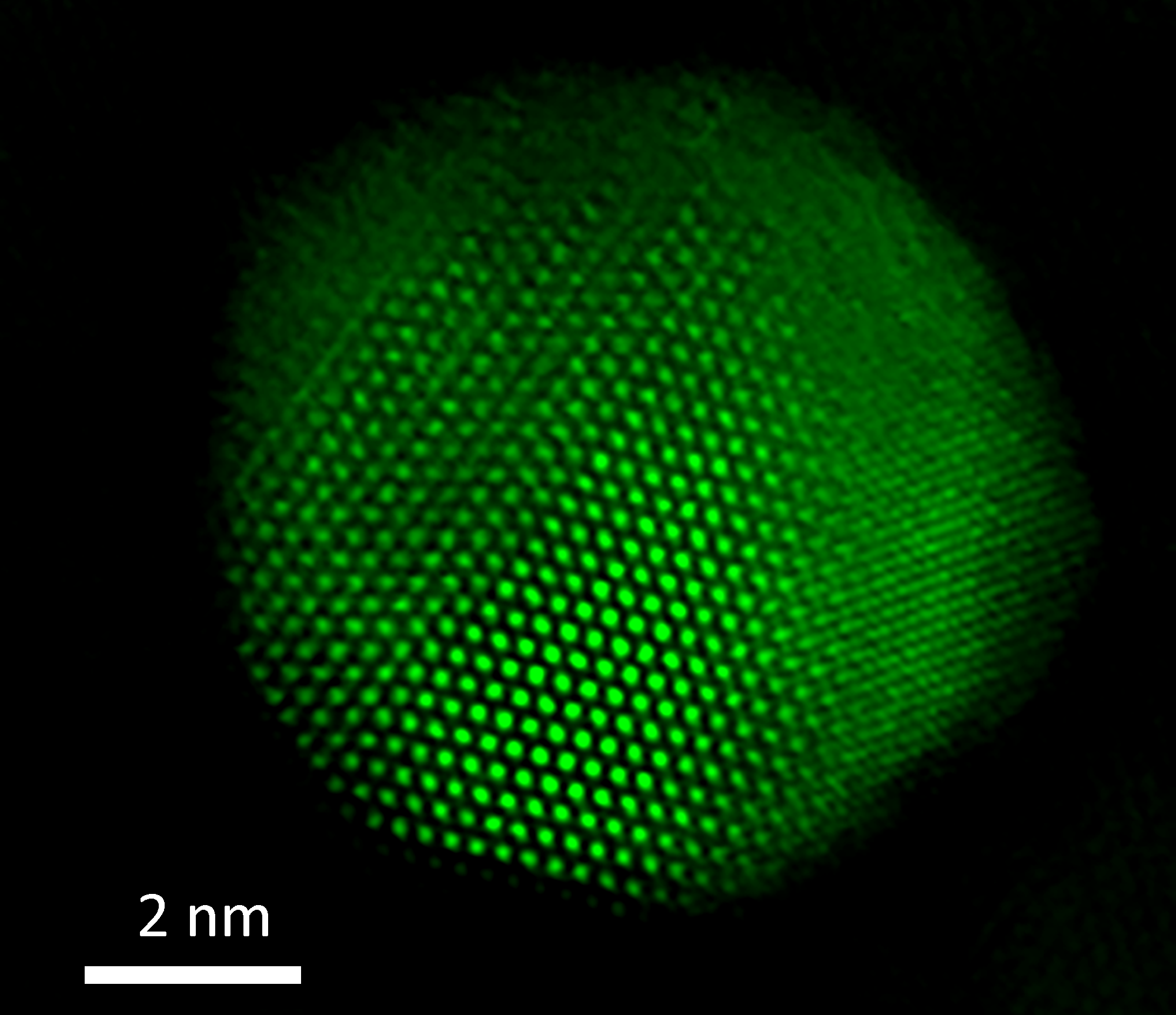
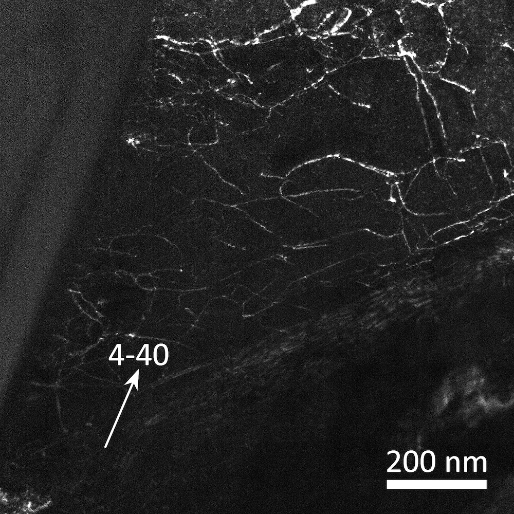
With TEM imaging (also in scanning mode, STEM) the sample material can be investigated in bright field and/or dark field mode. The range of magnification spans from features with the size of a few micrometers down to atomic resolution (HRTEM).

In-situ / operando TEM
In-situ and operando electron microscopy enables observation of materials under the influence of defined physical, electrical or chemical stimuli. It is possible to follow dynamic processes and make the important transition from imaging in vacuum to observation under relevant conditions.
ScopeM is equipped with various in-situ holders for heating up to 1000 °C in vacuum or in gaseous environment or for (electrochemical) experiments in liquids. more
Analytical (EDS and EELS)
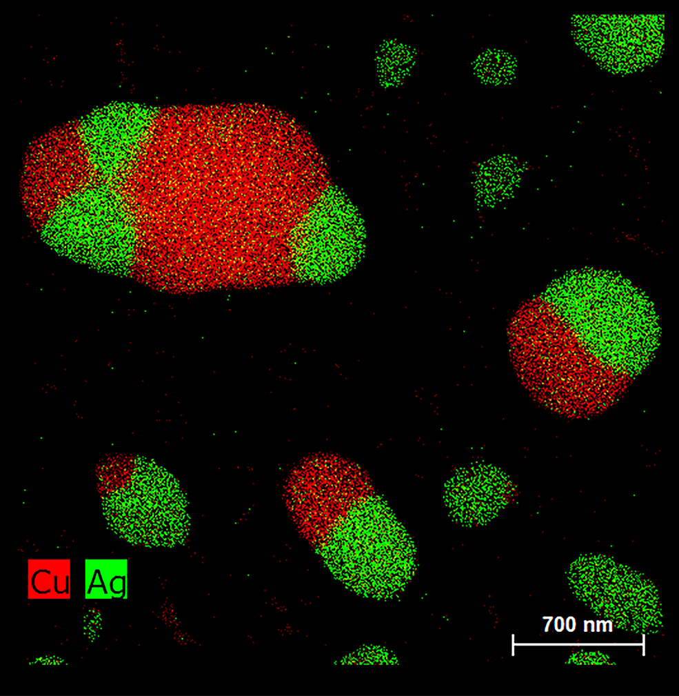
When the electron beam interacts with the sample, the energy of the electrons can be altered and X-rays can be generated. Both effects carry information about the elemental composition and the chemical characteristics of the sample. Electron energy loss spectroscopy (EELS) and energy dispersive X-ray spectroscopy (EDS) is used to exploit this information.
Tilt series/Tomography
By rotating the sample holder, the initially two-dimensional imaging can be expanded to the third dimension. A set of images, taken under changing tilt angles, can be used to reconstruct a tilt series, a three-dimensional image of the sample. more
Lorentz Microscopy
Lorentz transmission electron microscopy (LTEM) allows to visualize the magnetic domains of a material. It relies on the fact that the Lorentz force deflects the electrons passing through a magnetized region. LTEM is thus very sensitive to the magnetic components in the plane of the TEM thin foil and allows revealing the domain walls, which become clearer and clearer the larger the defocus.
Diffraction (SAED and CBED)
The periodic structure of a (micro-)crystalline material acts as a grating, scattering the incident electrons. The resulting diffraction pattern can be used to deduce the initial crystal structure.
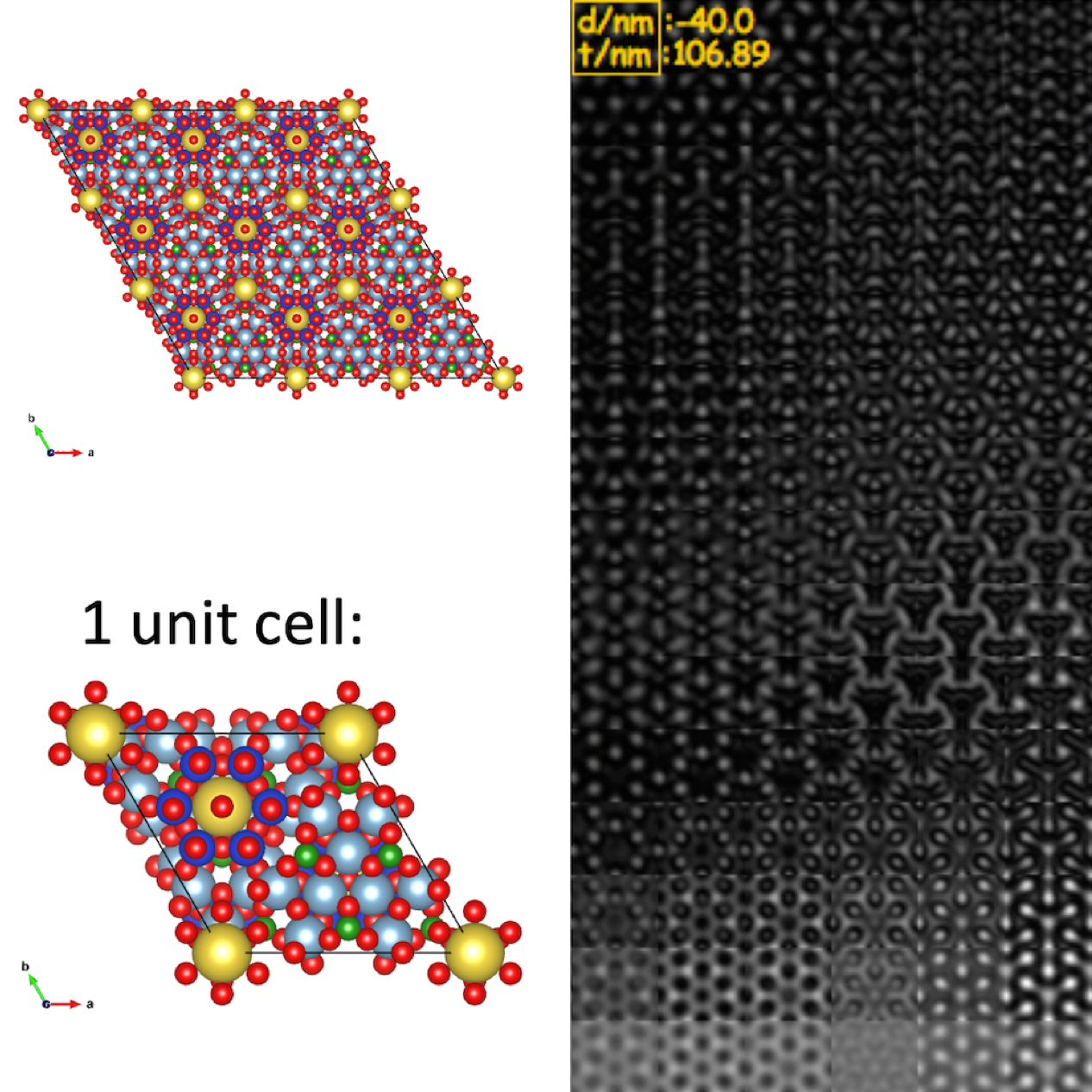
Image simulation and data analysis
Simulation of images and diffraction patterns based on structural models support the interpretation of experimental data.