Electron Backscatter Diffraction
Selected projects performed at ScopeM using in-situ techniques are listed below.
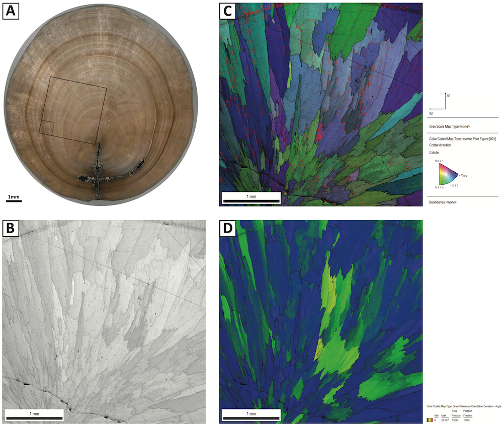
Electron backscatter diffraction is an analytical scanning electron microscopy technique that provides crystallographic orientation and microstructural information of crystalline samples. The images show examples of EBSD maps derived from a sample of Belemnite (a fossilized squid-like cephalopod - image A), including an image quality map (B), and orientation map (C) and a grain reference orientation deviation map (D).
More details of this sample can be found in:
Vickers, M. L., Bernasconi, S.M., Ullmann, C.V., Lode, S., Looser, N., Morales, L.F.G., Price, G.D., Wilby, P.R., Hougård, I.W., Hesselbo, S.P., Korte, C. 2021. Marine temperatures underestimated for past greenhouse climate. Scientific Reports, DOI: 10.1038/s41598-021-98528-1
by K. Kunze, A. Sologubenko, H. Ma and R. Spolenak
Abstract: MC Regensburg, August 25 – 30, 2013, DOI: 10.5283/epub.28734 (part 1, pages 744-745)
Crystallographic orientation mapping is usually facilitated by rapid indexing of electron backscatter diffraction (EBSD) patterns, also referred to as orientation imaging microscopy [1]. A suitably positioned semiconductor diode (forescatter electron detector) allows recording orientation contrast images with high angular sensitivity at the same SEM conditions. The spatial resolution of both complementary techniques is restricted by considerable scattering of the primary electron beam (with energy typically between 10 and 30 keV) at shallow incidence (around 20°) to the surface of bulk sample material. This measurement geometry results in an anisotropic interaction volume and subsequent resolution of about 20 nm by 50 nm [2].
Recently, a setup has been introduced for crystal orientation mapping on thin electron transparent sample materials by recording transmission Kikuchi diffraction (TKD) patterns using the conventional EBSD hardware and software [3,4]. Benefits of this approach result from a horizontal sample position, i.e. perpendicular to the incidence beam. The isotropic interaction volume in the thin sample foil enables to resolve grain boundaries at 10 nm mapping step distance.
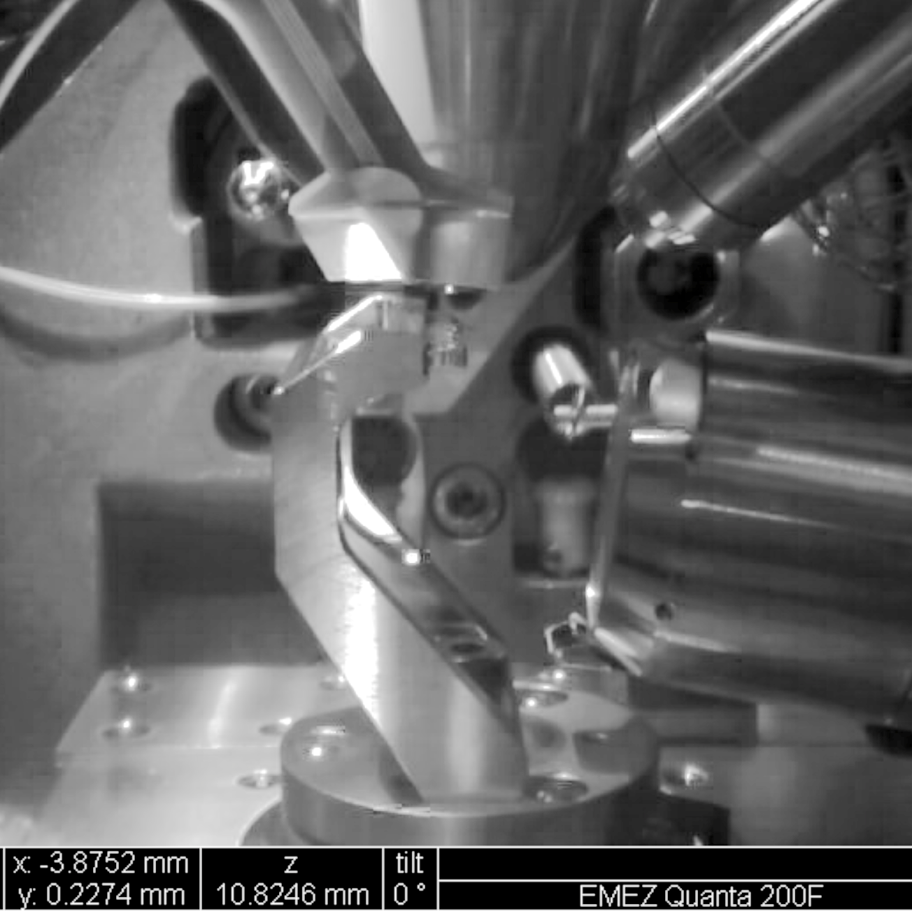
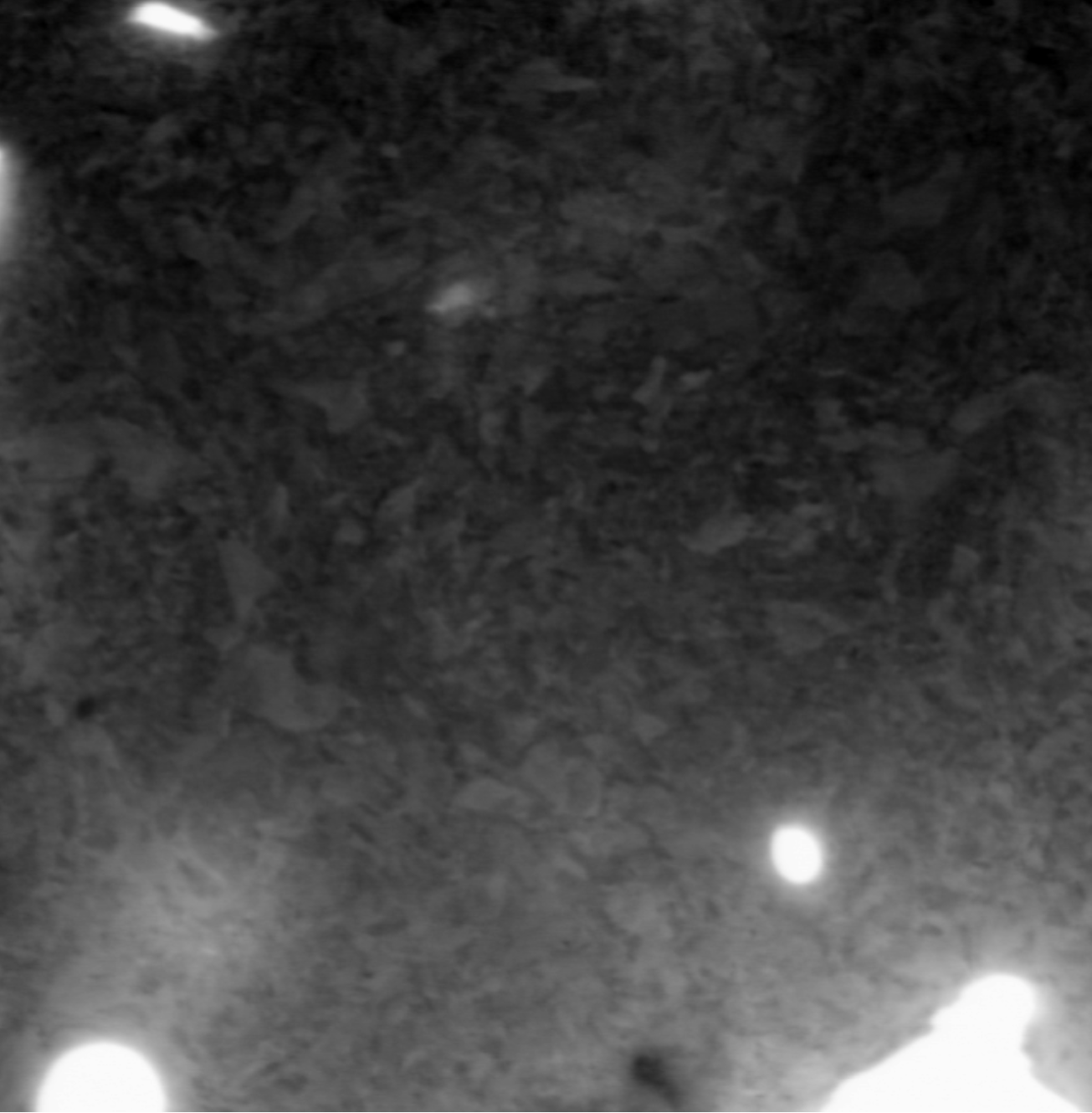
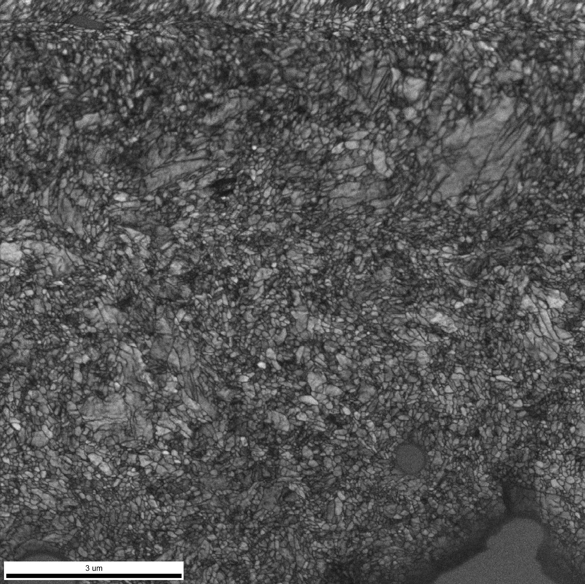
Here, we present a setup by commercial components of a SEM (FEI Quanta200F), a STEM sample holder (FEI) enabling a working distance of 5 mm, and an EBSD detector (Ametek-EDAX Hikari) with FSD diode attached (Figure1). The example shows a TKD mapping on nanocrystalline Titanium, with a map size of 10 μm x 10 μm at 10 nm steps. Only reliably indexed orientations (after some moderate data cleaning) are displayed in the colour-coded map (Figure 2), where the dominating bluish colours indicate strong crystal preferred orientations.

The microstructure consists of highly deformed grains with sub-micron sizes. All original data (without any postprocessing) are included in the mapping of TKD pattern sharpness (Figure 4). Grey level (qualitative) contrast arises not only from large angle grain boundaries, but also from higher dislocation densities. Holes in the thin foil are decorated by a narrow corona of poor diffraction patterns due to the extremely thin foil thickness (e.g. at the lower right corner).
Besides of crystal orientation mapping, orientation contrast imaging is facilitated by recording high angle dark field STEM images using a FSD diode, available with the EBSD detection system. The orientation contrast image corresponding to the map of Figures 2 and 4 is provided in Figure 3. A vast of detailed contrast is visible, which is only partly matching the contrast from the pattern contrast map. TEM studies of the intragranular defect morphology of nanocrystalline Titanium confirm a very high sensitivity of the TKD mapping to the subgrain structure and evidence the potential of TKD as a tool for the study of crystallographic relationships of nano-sized features.
[1] B.L. Adams, S.I. Wright, K.Kunze, Metallurgical Transactions 24A (1993), 819-831
[2] S. Zaefferer, Ultramicroscopy 107 (2007), 254-266
[3] R.R. Keller, R.H. Geiss, Journal of Microscopy 245 (2012), 245-251
[4] P. Trimby, , Ultramicroscopy 120 (2012), 16-24